Sony’s newest sensor captures twice the light
The world's first two-layer transistor pixel design enables wider dynamic range and lower noise levels. And it's coming to a camera near you.
We may earn revenue from the products available on this page and participate in affiliate programs. Learn more ›
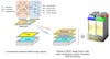
Earlier today, Sony’s semiconductor division announced the development of the world’s first stacked CMOS imaging sensor with two layers of transistor pixels. This new design is significant because it doubles the sensor’s light-gather capability compared to a traditional stacked CMOS sensor.
More room for photodiodes and transistors alike
By moving most of the transistors to a different layer of the silicon substrate from that used for light gathering, Sony has been able to greatly increase the area given over to each photodiode. The result is a doubling of the signal saturation level, or the maximum number of electrons that can be stored at each pixel location.
At the same time, by moving most transistors to their own layer, the individual size of each can also be increased. And not surprisingly, this is exactly what Sony has done.
Lower noise levels and better dynamic range
Related: Canon’s news sensor sees color in the dark
So what does all of this mean for image quality? Well, by improving the sensor’s saturation level, Sony has also increased the dynamic range of the chip, or in other words, the range from the darkest to brightest levels that it’s capable of registering. And by enlarging the amp transistors, it has simultaneously reduced output noise levels.
It’s important to note that while the signal saturation level has been doubled, that doesn’t necessarily translate directly to a doubling of dynamic range. (And nor does it imply a halving of noise levels.) Other factors of the sensor design will also have their part to play, and Sony has yet to quantify the scope of the DR or noise improvements it has achieved.
Look for the tech in smartphones and small-pitch sensors first
Still, it’s clear that there’s the potential for a big step forward in both respects. We’d expect this news to have the greatest impact on smaller, higher-resolution sensors like those used in smartphones, before making its way to larger sensors, as was the case when backside-illuminated sensor designs first went mainstream.
With less area available to each photodiode in the first place, the potential for improvement in a small, high-res sensor is greater than it would be in one with low resolution and/or a large surface area. And Sony suggests as much itself, noting that its tech will allow “the realization of increasingly high-quality imaging such as smartphone photographs”.
When will it be available?
Sony has yet to announce any products based on the new design. Nor has it thus far offered any timeline for its potential commercialization of the tech. But we’ll certainly keep a watch for any updates and report back accordingly.
