New Gear: Sony Redesigns the Backlit CMOS for Cellphones
Sony has developed a new backlit CMOS sensor, which promises better low-light performance in less space.
A new development from Sony means better imaging sensors might be making their way into smaller devices — and the company is promising less noise and better low-light photography. The newly announced back-illuminated CMOS image sensor moves all the circuitry for the chip beneath the image sensor itself, dramatically reducing the component’s footprint. The circuitry now functions as the support structure, and allows a better sensor to take up less space.
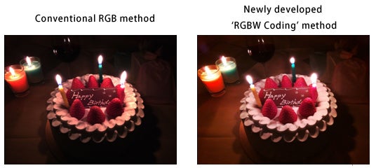
In addition to improving the size of the chip, Sony is also promising higher image quality, faster speeds, and lower power consumption. Sony has also announced two examples of what the stacked CMOS chip can do, “RGBW Coding” and “HDR Movie”. “RGBW Coding” adds white pixels to the sensor, which ups low-light performance, and Sony claims to have defeated the lower image quality that can accompany this feature. The “HDR Movie” functionality allows for multiple exposure levels within a single frame of video.
The company plans to ship a 1/4-inch, 8MP sensor without the cool new modes in March, a 1/3.06-inch, 13MP version with “RGBW Coding” and “HDR Movie” in June, and an 8MP, 1/4-inch sensor with both features in August.
[via DPReview]